
Optical Networking Primer
AI infrastructure's new bottleneck

Since late 2022, a good way to make money in tech has been to identify bottlenecks in the AI supply chain and invest there. Optical networking businesses have long been thought of as telco-cyclical, commoditized hardware players. While the cyclicality hasn’t gone away, increasing performance demands of AI-optimized datacenter architecture is rapidly changing the importance of optical components and improving the value capture of key players. Optical networking’s share of DC capex looks set to expand from a low-single-digits % driven by three architectural shifts that are a “when not if.”
When I started writing this note, I had intended to publish a TAM forecast as my output - it’s a logical break - before moving into specific companies. I realized however that my process is iterative and my numbers would likely change significantly after posting. As a result, I’ve documented how I’m framing it and the qualitative factors I’m considering - but will withhold my explicit estimates.
I want to thank everyone who has helped me ramp on optical either by sharing notes or speaking with me [names omitted to respect people’s privacy].
I. The Physics of Optics vs. Copper
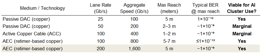
The trade-off between reach and power illustrated above highlights why interconnects are shifting toward optical solutions as bandwidth demands scale. The leading edge of data center compute is rapidly approaching the copper wall. In copper (Cu) transmission, there is an inverse relationship between lane rate and max reach. As lane rates move toward 224G and beyond, the electrical signal degrades so significantly over distance that Bit Error Rates (BER) exceed manageable thresholds for the physical layouts required in modern high-density AI clusters.
As of 1CQ26, Optical use for 800Gb/s is still growing and 1.6Tb is already ramping but we are still very early. I think CREDO mgt. has estimated that 95% of interconnects today are still copper.
In my mind the above table is sufficient to conclude that as lane rates continue to increase, optical networking will continue to replace Cu. There are other reasons why the industry will eventually move to optics and some very technological real hurdles to overcome which I’ll discuss later but these relate to “when” not “if.”
II. Demand Drivers
The majority of incremental demand optical networking will be driven by growth in inference and training compute.
Additional compute obviously translates to higher datacenter capex related to AI clusters:
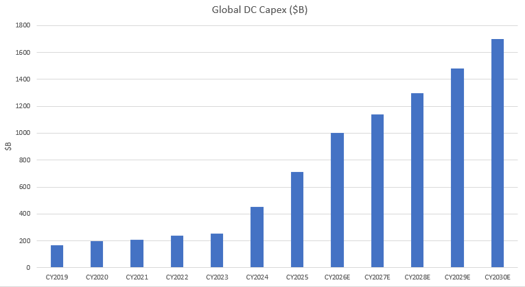
Above is my simple forecast loosely based off recent Dell’Oro estimates where I have total DC capex increasing by 2.4x over the next 5 years. Given the 2 year lead-times on building datacenters, near term consensus is decent. 5 year out estimates vary a bit more.
The upper bound [not shown] is constrained by numerous supply chain bottlenecks over the next few years. The lower bound [not shown] is constrained obviously only by our imagination. There are many possible scenarios where spend is lower 5 years out.
A DC capex estimate is critical to estimating future earnings of optical supply chain companies. While I watch this very closely, I don’t want to spend time in this post debating it.
Ultimately, some portion (my 2025 estimate: LSD %) of that capex is indirectly spent on optical networking. Absent any other changes (of which there are many), I would expect datacom end market demand for optical networking to roughly increase by 2.4x.
III. Network Architecture
This section lays out the observations that lead me to conclude that optical networking will outgrow total DC capex.
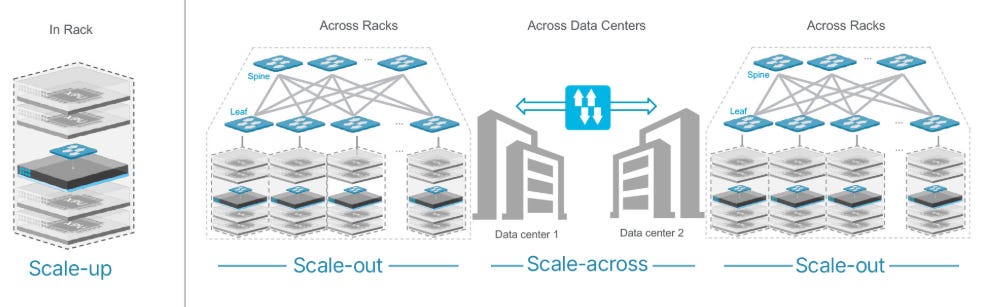
Listed in order of potential:
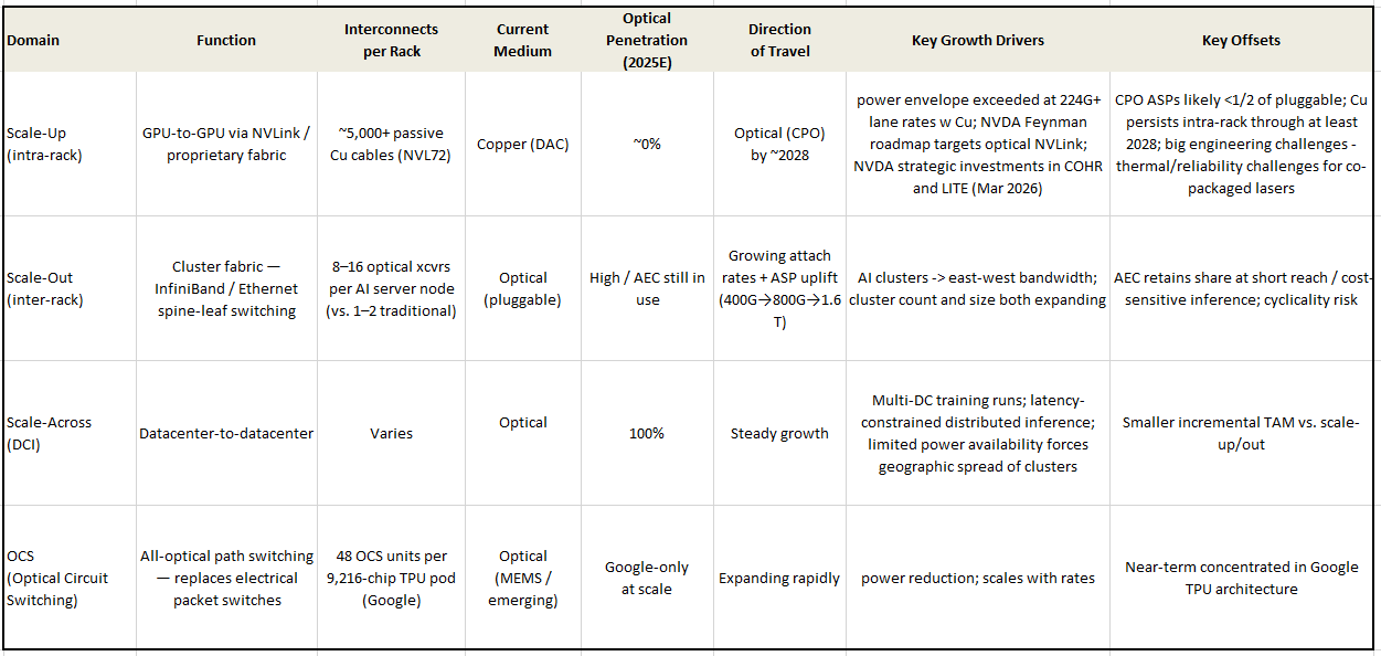
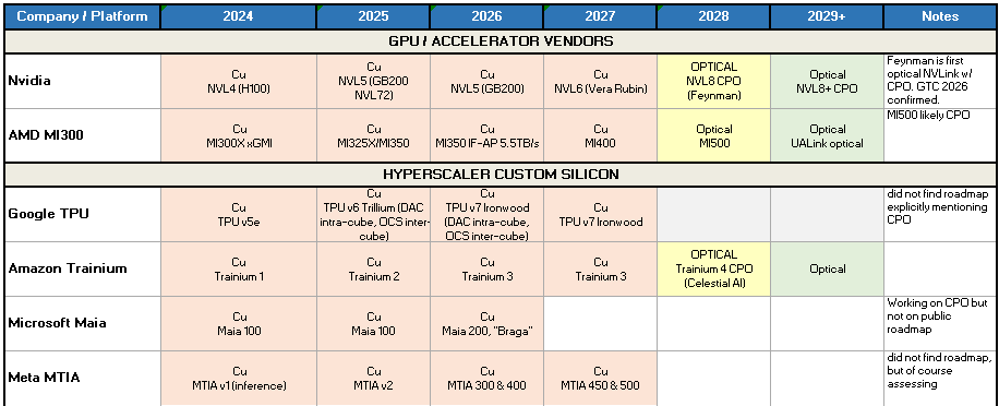
Scale-up (intra-rack interconnect) is copper today. There are approximately 10x as many intra-rack interconnects as inter-rack interconnects in a datacenter today. A NVL72 uses 5.2K passive Cu cables. As rates rise, the cables begin to require active conditioning (AEC) and the implied watts per cable exceeds the power envelope of the entire server: optical interconnects seem mandatory to me. Hence NVDA's roadmap for Feynman (currently slotted for 2028) is looking to move to optical NVLink with CPO [see Mar. 2, 2026 capacity investments NVDA → COHR and NVDA → LITE]. In addition to NVDA, every other major accelerator vendor and CSP ASIC designer is taking a serious look.
The offset: CPO would carry a lower ASP (<1/2 vs pluggable?), which is crucial for TAM modeling—higher module density × lower price per module = faster adoption and higher revenue despite per-unit price compression.1
Here’s my current incomplete tracker. CPO options are already available from AVGO (I remember watching their Silicon Photonics presentation in 2021). Scale-out and Scale-across. This is the historical optical DC TAM.
Scale-out. Inter-rack connections in an AI cluster use optical transceivers or AEC. The TAM here looks very exciting to me for two reasons: first AI-focused datacenters move data around internally to a much greater degree than traditional workloads, and second generational upgrades are accompanied by ASP increases.
First In a traditional datacenter, servers are largely independent — a web server handling requests doesn’t need to constantly synchronize with the server next to it (you’ll hear this referred to as North-South vs East-West data traffic). The networking fabric exists primarily to connect clients to compute, not compute to compute. A rough rule of thumb: 1–2 optical ports per server.
In AI training clusters large models are spread across multiple processors in a cluster which must participate in collective operations. A GPU that can’t communicate fast enough becomes the bottleneck for the entire job.
A single B200 server (typically 8 GPUs) connects to the fabric through multiple high-speed uplinks for scale-out as well as storage and CPU fabric. That’s 8–16 optical transceivers per server node, versus 1–2 in a traditional workload. Consider also that the clusters are growing in both number and size.

Source: Gemini. Illustrative only — directionally correct, not precise. Second The generational upgrade cycle that we see in most hardware components is additive. Each generation: (400G → 800G → 1.6T) roughly doubles port bandwidth while ASPs increase before eroding as the generation matures. Growing attach rate + cluster count growth + historical generational ASP = scale-out optical revenue growth structurally outpaces headline DC capex.
Offset: AEC (Active Electrical Cable) will keep some share in scale out. AEC uses active signal conditioning to extend copper reach to ~3–5 meters, enough to cross a rack or reach a top-of-rack switch. AEC should remain competitive particularly for cost-sensitive inference.
Scale-across (DCI) is a smaller but higher-ASP market. This addresses moving data not within a datacenter but between datacenters. Given the longer distances, this has long been the domain of optics and I currently think should be a smaller growth driver. As a result, I’ve tabled my analysis here and moved on.
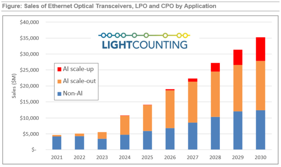
Here’s a TAM estimate by LightCounting showing (in the historicals) how AI is changing demand:

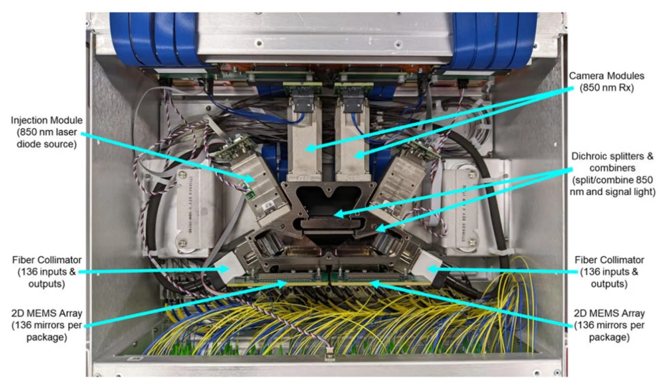
Optical Circuit Switches (OCS)
A typical switch converts photons into electricity and then back into photons. An OCS currently employed only by GOOG to link TPUs keeps the data as photons. Amazingly (to me), these switches are rapidly reconfigurable as well which seems highly advantageous. The switching technology here is MEMs based. I need to learn more about OCS before I’d be willing to make an estimate as to the ultimate effect this could have on the TAM. Lightmatter which is currently private ($850M funding, $4.4B valuation) has an interconnect solution as well - very interested in digging in here.

Source: Google via https://www.datacenterdynamics.com/en/analysis/mission-apollo-behind-googles-optical-circuit-switching-revolution-mag/
IV. Technology Landscape
The debates and questions in this section are why a TAM estimate is tough. The outcomes and timing have meaningful implications for which companies capture value. After reading this, please let me know if you think I’ve missed anything.
A. How Fast Does the Industry Move to Co-packaged Optics (CPO)?
CPO is an inevitable necessity for scale-up. Will it hit in 2028 as the industry thinks or be pushed out? Near-packaged Optics (NPO) (OBO in the image below) are in implementation today but I think cannot be a stopping point because while it shortens the electrical path, it doesn’t eliminate it and hence doesn’t solve the system constraints even short Cu distances impose.
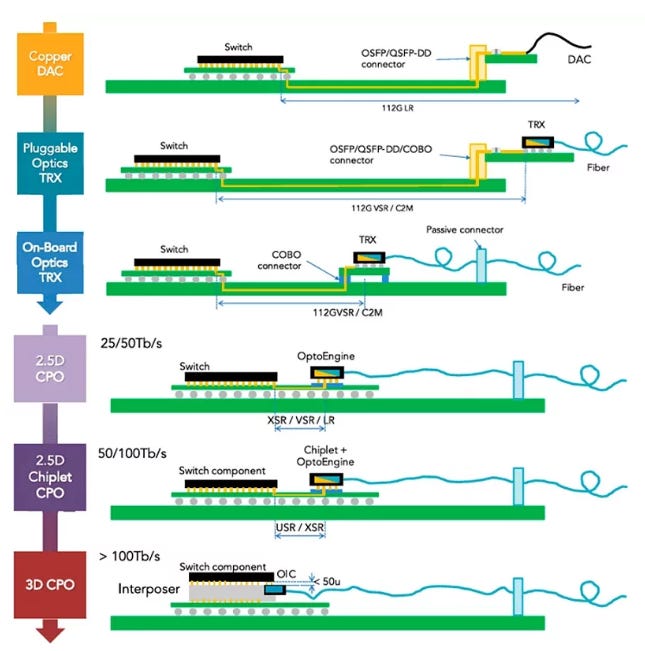
The above is a helpful graphic which illustrates the technological progression from “dumb” Cu to CPO and how hard Cu is to use at higher rates.
While Cu is surely hitting its limits, deployment of CPO requires jumping technological hurdles to achieve the promised power savings.
First, lasers have higher failure rates. Sticking it on an expensive GPU means when the laser fails, the chip will be out of commission for much longer.
Second, transistors are still Cu and generate lots of heat. Lasers are temperature sensitive. Packaging the two together will require thermal solutions that haven’t been rolled out in HVM yet.
There are many other non-trivial engineering problems related to both yield at high volume and actual implementation, but I believe these are the biggest today.
In CPO, pluggable modules COHR and others sell go away. While COHR and LITE would maintain a strong position in lasers, the development of the Silicon Photonics die is a land grab. Currently AVGO has the most mature SiPh technology. I also hope to meet and learn more about Ayar Labs.
B. Photonic Platforms
B1. An Overview of Platforms
Currently the most likely approach for CPO is a hybrid SiPh + InP. These simplify the role of the InP based device to light generation and reception.
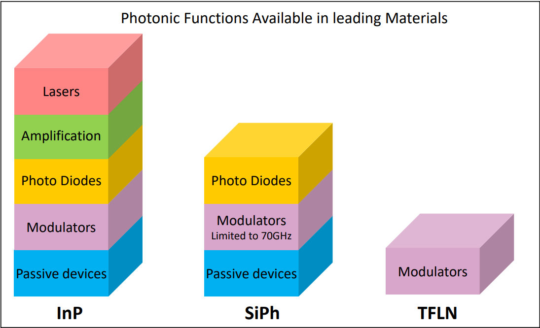
The shape of these future devices (which integration scheme will become the standard) is being hashed out by the industry.
SiPh involves building light modulation functionality on traditional silicon wafers but requires an external light source (InP used to make a CW laser). It wins at scale on cost because the industry is already very good at most of the required manufacturing steps and has tons of collective process knowledge (12 in. CMOS fabs).
Using Indium Phosphide (InP) wafers allows for the generation and modulation of light in one device. This is used today in EML lasers and transceivers today - it is the domain of LITE and COHR currently - and enjoys a performance edge.
B2. Integration Schemes
Hybrid SiPh + InP encompasses a few potential solutions ad the industry has not converged on a standard. This is an interesting area to learn about - if I can become convinced that one particular technology will prevail, I might be able to identify an equipment supplier that would stand to benefit. The hybrid approach limits the functionality built on InP wafers.
My current understanding is that a few approaches are being pursued: Butt-coupling, and heterogeneous bonding are the two front runners.
Putting It Together
Three observations lead me to conclude that the optical TAM will outgrow DC capex over the medium term:
Largest pool of interconnects is 100% copper today. Scale-up interconnects outnumber scale-out by roughly 10:1. Physics makes this untenable beyond 224G lane rates as the power necessary to condition the signals (retimers) exceeds the envelopes of the servers.
AI network architectures are multiplying optical attach rates per server. While a traditional server requires 1-2 optical ports, an 8-GPU server might require 8-16. As both the number and size of AI clusters grow, optical attach rates compound on top of server units.
Generational transitions will continue to be ASP-accretive.
My current research outline is to tackle unit economics across architectures, supply chains and competitive dynamics, and then how I can best forecast a TAM. I am very interested in how much value accrues to the optical players and who is likely to capture it. If CPO arrives on schedule, pluggable module revenue shifts to SiPh and laser supply with lower ASP but huge volumes.
If you have any data points or pushback that could improve my understanding of the space, I’d really welcome it - please reply here or reach out directly.
As an investor, my work jumps from here to specific companies to see what’s already priced in.